Example SAS design guide with Helinks STS
Substation
The substation is called IOP. You can find more information about it on this link: Example SAS design with Helinks STS
The focus of the guide will be recreating three bays of the IOP substation and configuring the communication exchange between their IEDs and finally exporting the SCD file.
As you can see from Figure 1, the following bays are created in this guide:
Incomer A: IncA1
Incomer B: IncB1
Tie breaker: BT1
To speed up the process, some power equipment have been excluded from the single line diagram.
Each phase of the design is explained in detail in the guide and instructions are given to create Specification and Integration for the IOP substation. Specification is about drawing the single line diagram and function specification. Integration revolves around importing and implementing IEDs to the system, configuring communication applications, and exporting the SCD file.
the starting point of the example project can be downloaded in the attachment link below.
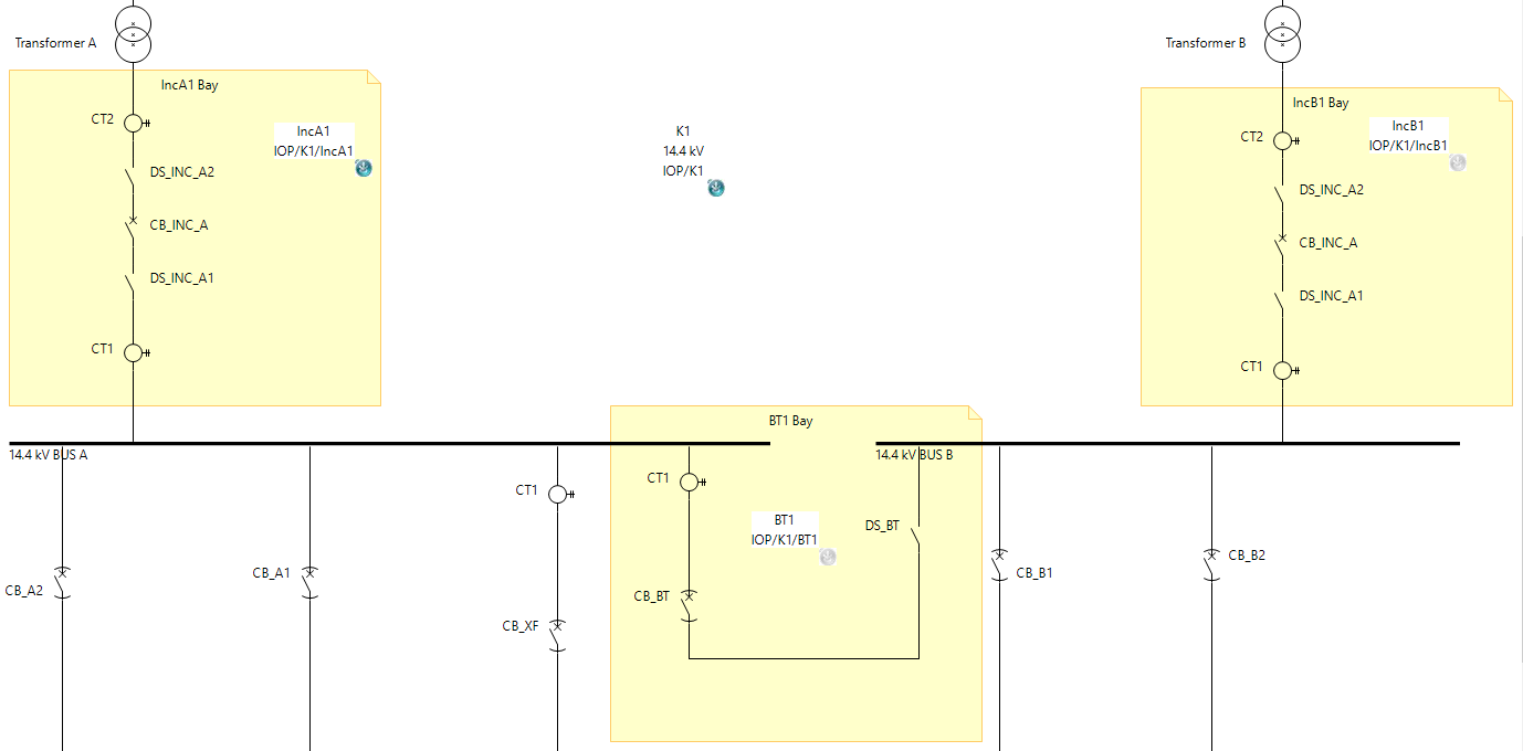
Figure 1: IOP Substation, LV side
System Specification
Specification part of the design focuses on designing the single line diagram and function specification in the substation.
Single Line Diagram
The single line diagram of the substation is shown by opening the Single Line functionality from the HELINKS STS dashboard.

The right side of the screen shows the palette. Each tab helps in drawing the single line diagram according to the IEC 61850 hierarchy. Design of a substation single line diagram can begin with specifying the substation name and voltage level name using “Substation” and “Voltage Level” under “Substation Structure”. Each voltage level can have one or multiple bus bars and bays using the two options under the “Bus and Bus Bar” tab. Finally, each bay can have different power equipment which can be chosen from the “Power Equipment Library” tab.
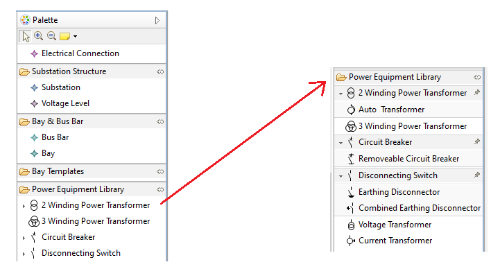
Figure 2: Single Line Diagram Palette
The IOP substation in the “IOP2019_DemoStart“ does not have the three bays and looks like the following figure.
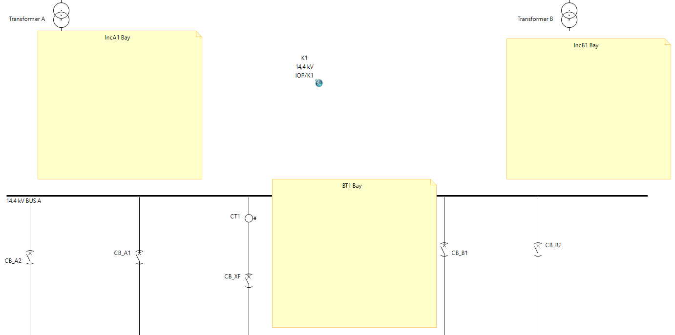
Figure 3: IOP Single Line Diagram without bays
The power equipment which are missing from each bay are listed in the table below:
Table 1: IOP Power Equipment list
Bay | Power Equipment | Number of equipment | Equipment name |
IncA1 | Current Transformer | 2 | CT1 CT2 |
Disconnecting Switch | 2 | DS_INC_A1 DS_INC_A2 | |
Circuit Breaker | 1 | CB_INC_A | |
IncB1 | Current Transformer | 2 | CT1 CT2 |
Disconnecting Switch | 2 | DS_INC_B1 DS_INC_B2 | |
Circuit Breaker | 1 | CB_INC_B | |
BT1 | Current Transformer | 1 | CT |
Disconnecting Switch | 1 | DS_BT | |
Removable Circuit Breaker | 1 | CB_BT |
Instructions
Open HELINKS STS and choose the correct workspace. (IOP2019_DemoStart - IOP2019)
Click on Single Line from the Dashboard to open the single line diagram.
Make sure the voltage level K1 which is the lower voltage level of the substation is highlighted and then create the two of the three missing bays according to the information from Table 1 and shown in Figure 1. Name them the same shown in the highlighted areas: IncA1, IncB1, and BT1.
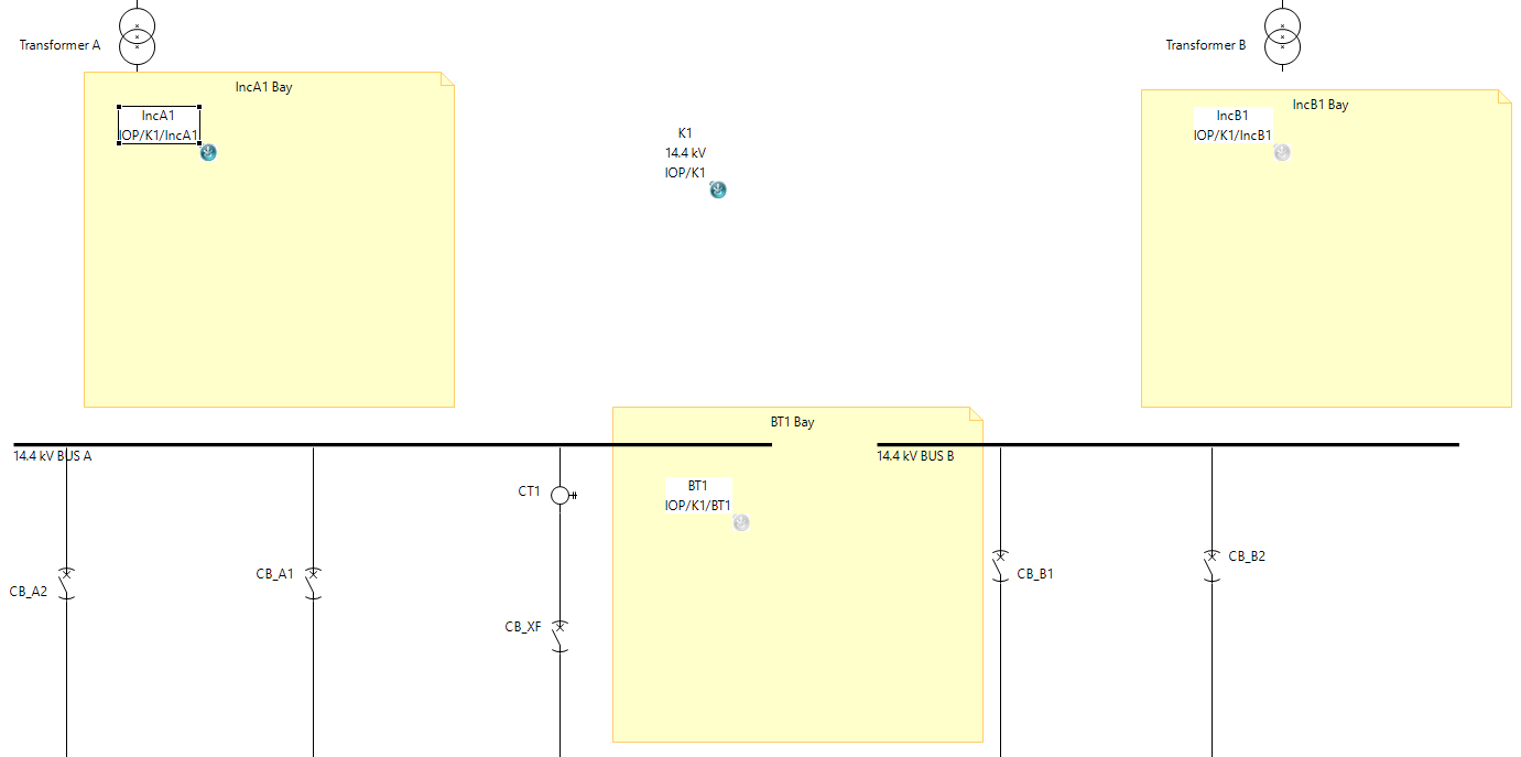
Figure 4: IOP bays without equipment
Figure 4 shows the bays which are created. According to Table 1, it is known which power equipment should be used for each bay.
Very Important Note: For placing equipment in the screen, you need to make sure you are placing them for the appropriate bay. Simply click on the bay to highlight it and then click on the power equipment and click on the screen.
Make sure the bay IncA1 is highlighted. You can do it by just clicking on the bay.
Click on the Current Transformer block from the library and click on the screen. Name it CT2. Create another one and call it CT1.
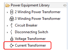
Figure 5: CT in power equipment library
Then create two Disconnecting Switches by clicking on its icon and naming them according to Table 1.
Place a circuit breaker in the screen for IncA1 by clicking on Circuit Breaker from the library and clicking on the screen. Use the name from Table 2.
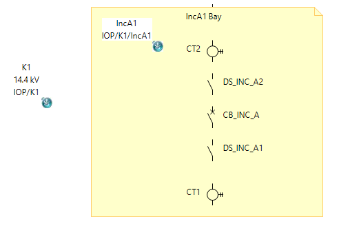
Figure 6: IncA1 equipment
Figure 6 shows all the power equipment for IncA1 bay.
In order to validate the equipment have been placed for the correct bay, use the right mouse click on the bay IncA1 and choose “Select Children”.
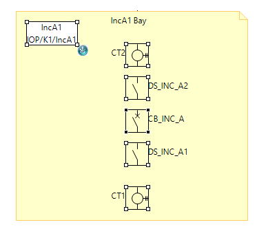
Figure 7: IncA1 Equipment validation
Lastly, click on “Electrical Connection” from the palette, shown in Figure 2, hover the mouse curser over one of the equipment and hold the mouse left button and draw a line between that equipment and another one and they can connect to each other. Make sure CT1 is connected to busbar 14.4kV BUS A and CT2 is connected to “Transformer A”. This creates the connectivity nodes and terminals and finishes the single line diagram part for this bay.
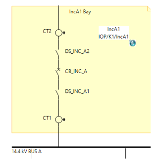
Figure 8: IncA1 with equipment and connections
The bay IncB1 is identical to IncA1 so place the same equipment for IncB1.
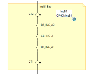
Figure 9: IncB1 with equipment and connections
You can follow the same instructions and create the single line diagram for BT. Click on the bay BT1 and make sure it is highlighted.
Remember to look at Figure 1 and Table 1 for reference. BT1 has a removable circuit breaker. You can choose it from the power equipment library and expanding the options for circuit breaker.
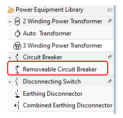
Figure 10: Removable circuit breaker from the library
Remember to connect all the equipment to one another and to the 14.4 kV BUS A by using Electrical Connection.
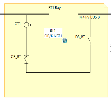
Figure 11: BT1 bay with equipment
Function Specification Diagram
Specification related to types of functionalities of each bay and its IEDs are created in the function specification diagram for bays in Helinks STS. As an example, we will attempt to create the specification for IncA1.
You can open the function specification diagram for each bay by double clicking on arrow pointing down icon next to the bay.
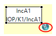
The function specification diagram of bay IncA1 can be opened by clicking on the icon as shown above.
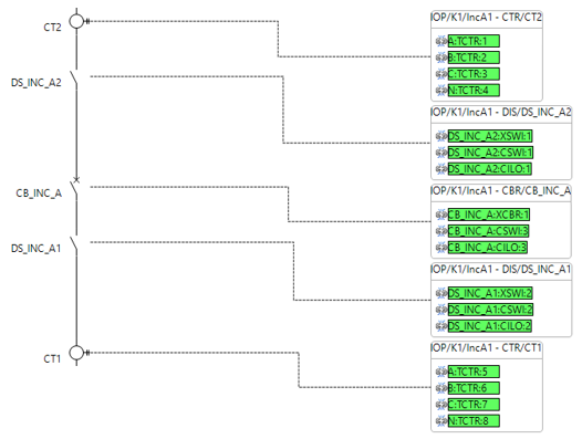
Figure 12: Function Specification Diagram of bay IncA1
Figure 12 shows the control functions that are created for the power equipment for bay IncA1. This is done automatically by Helinks STS whenever an equipment is created in the single line diagram. The control functions contain appropriate control and monitoring logical nodes for each equipment. For example, the function for the circuit breaker CB_INC_A contains the logical node XCBR (breaker status), CSWI (breaker command), and CILO (interlocking).
On the right side of the screen, you can see different options for function specification for the bay.
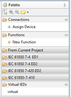
Figure 13: Function Specification Diagram tabs
Functions: The “New Function” from this tab can be used to create additional functions for each bay. It also houses any functions which are saved to the HELINKS STS function library.
IEC 61850 7-4 ED1, ED2, 7-420 ED2, 7-410: These are the collection of logical nodes based on IEC 61850-7 data model grouped under their names. For this project, the 7-4 ED2 logical nodes are used.
Virtual IEDs: The “virtual” option from this tab can be used to create virtual IEDs in the function specification diagram.
Connections: The virtual IEDs are assigned to functions using the “Assign Device” from this tab.
By using the palette, users can create additional functions and choose different logical nodes for each and finally assign virtual IEDs to functions. The bays in this project have bay protection and control units and merging units.
The following tables show the functions which are created for power equipment and additional functions for each bay. They also specify the virtual IEDs which are assigned to each function.
Table 2: IOP power equipment function specification
Bay | Power Equipment | Function name | Virtual IED |
IncA1 | Disconnecting Switch | DIS/DS_INC_A1 | PUBCU |
Disconnecting Switch | DIS/DS_INC_A2 | PUBCU | |
Circuit Breaker | CBR/CB_INC_A | PUBCU | |
CT2 | CTR/CT2 | MU | |
IncB1 | Disconnecting Switch | DIS/DS_INC_B1 | PUBCU |
Disconnecting Switch | DIS/DS_INC_B2 | PUBCU | |
Circuit Breaker | CBR/CB_INC_B | PUBCU | |
CT2 | CTR/CT2 | MU | |
BT1 | Disconnecting Switch | DIS/DS_BT | BCU |
Removable CB | CBR/CB_BT | BCU | |
CT1 | CTR/CT1 | MU |
Table 3: IOP Additional function specification
Bay | Function | Logical Node | LN Instance | Virtual IED |
IncA1
| Protection | PTOC | 1 – 3 | PUBCU |
| PTRC | 1 | PUBCU | |
BF | RBRF | 1 | PUBCU | |
IncB1
| Protection | PTOC | 1 – 3 | PUBCU |
| PTRC | 1 | PUBCU | |
BF | RBRF | 1 | PUBCU | |
BT1
| Protection | PTOC | 1 – 2 | PU |
| PTRC | 1 | PU | |
BF | RBRF | 1 | PU |
Table 2 and Table 3 show how the role of protection and control is assigned to one IED for the bays IncA1 and IncB1 while for the bay BT1, those roles are assigned to separate IEDs.
Instructions
In the function specification diagram for IncA1, click “New Function” and click on the screen to create two new functions. One of them is called “Protection” which handles the overcurrent protection and tripping functionalities. The other is called “BF” which is for breaker failure protection.
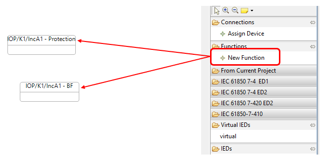
Figure 14: New functions for IncA1
Open the IEC 61850 7-4 ED2 library and choose “PTOC” under the “P - Protection Functions” group. Click on PTOC and click on the inside of “Protection” function which you have placed before.
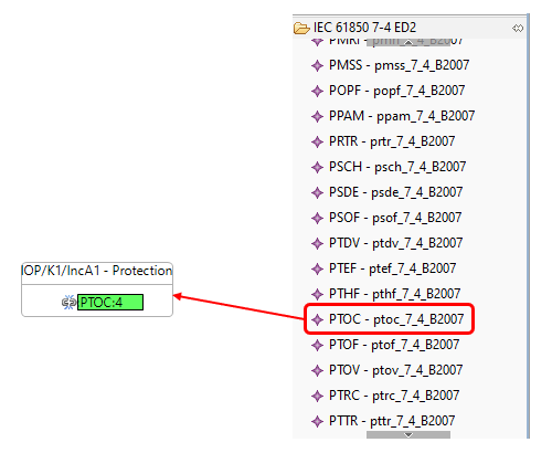
Figure 15: PTOC from IEC 61850 7-4 ED2
Create two more instances of PTOC by click on the logical node from the library and clicking on the “Protection” function. Create an instance of PTRC from the same “Protection Function” group from the IEC 61850 7-4 ED2 library and place it in the same “Protection” function.
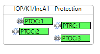
Figure 16: Protection function
Choose the logical node RBRF from the IEC 61850 7-4 ED2, under the group “R – Protection Related Functions” and click on the inside of the BF function.
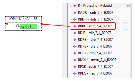
Figure 17: RBRF from “R - Related Protection Functions” in IEC 61850 7-4 ED2
The additional functions are created, and we can now create virtual IEDs to specify what each IED should do. Choose “virtual” under “Virtual IEDs” from the menu on the right-hand side of the screen and click on the screen. This virtual IED is named PUBCU. Create another one with the name MU.
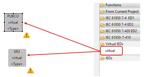
Figure 18: Creating virtual IEDs
PUBCU should be assigned to all the protection and control functions. MU is the merging unit and should be assigned to instrument transformers. Under the “Connections” tab, choose “Assign Device”. Hover the mouse button which has the arrow icon over the virtual IED PUBCU, hold the left mouse button and draw a line to the title of the function “Protection”.
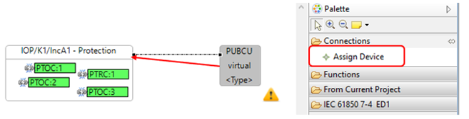
Figure 19: Assigning virtual IEDs to functions
Do the same method and assign PUBCU to all protection functions and power equipment functions, except the one for CT. Assign MU to the functions for CT2. The CT1 function is for another merging unit which is not featured in this guide and SCD file.
You can arrange all icons and straighten the lines by clicking on the icon “arrange all” once and twice.
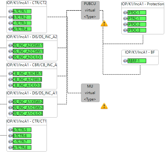
Figure 20: IncA1 Function Specification with virtual IEDs
Helinks STS adds some default signals for most of the logical nodes in the library but does not for some of the others like PTRC. So, we must specify signals for this logical node. Use the right mouse click on PTRC and choose “Configure Signals”.
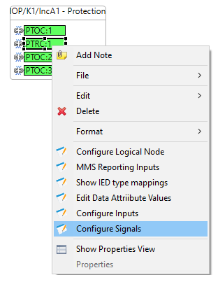
Figure 21: Configure signals for PTRC
Click on “Edit” on the page which opens. This opens another page which is the complete set of signals for this logical node according to the HELINKS STS IEC 61850 7-4 ED2 library. The available signals might differ once the IED is implemented and you are choosing signals from the IED data model.
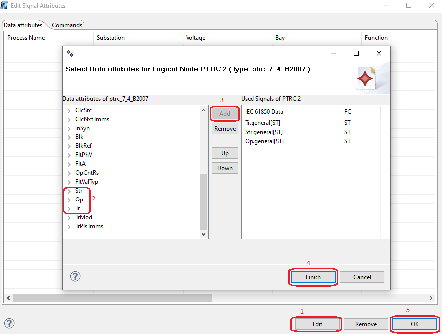
Figure 22: Adding signals for PTRC
We don’t know which IED is going to be implemented yet so we don’t know the data model. So, we can specify all the possible signals the IED data model might contain for PTRC logical node. Expand, Op, Str, Tr data objects and choose the signal with the data attribute “.general” for each one and click on Add to add the attribute to the “Used Signals” list on the right side. Click Finish when it is done and OK. Look at Figure 28 for reference since it shows the steps of the process.
Configure signals for RBRF and choose OpEx.general as shown in Figure 23.
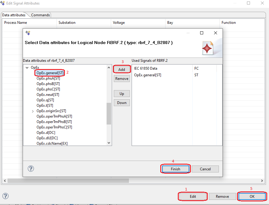
Figure 23: RBRF signals
Lastly, you must add signals for TCTR logical nodes as well. Follow the same method and add “AmpSv.instMag.i” data attributes for these logical nodes for all 4 instances.
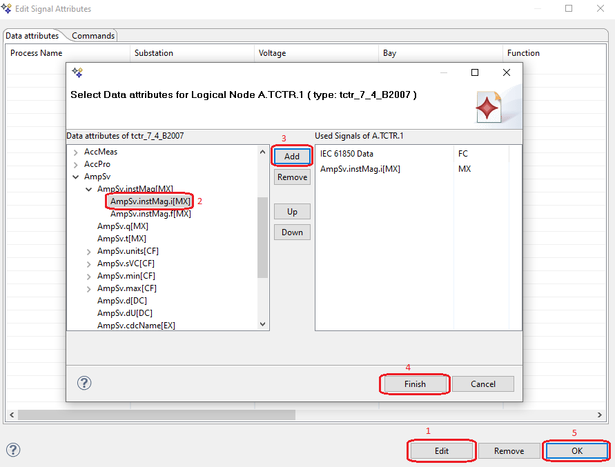
Figure 24: TCTR signals
Check the signals for PTRC by clicking on the logical node and clicking on “Signals” at the bottom of the screen
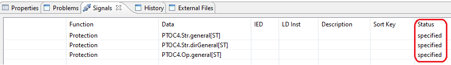
Figure 25: Signals for PTRC
Figure 25 shows the signals tab which contains the IEC 61850 address of each signal and their status which in this phase, is “specified”. You can check out the signals for the bay by clicking on the screen or you can see the signals for the whole substation by moving back to the single line diagram and clicking on the “IOP” substation name.
Optional: You can also add descriptions or even change signal names to distinguish between phases for example. You can try it for the measurement points on TCTR signals. Simply click on the “Description“ column or “Process Name“ and you can change the signal names to something more relevant to current measurement like “Phase A Current“. View the picture below.

The bay IncB1 is identical to IncA1 so follow the same instructions and create the functions, virtual IEDs, and signals for IncB1.
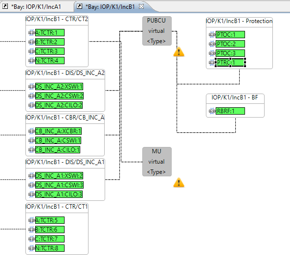
Figure 26: IncB1 Function Specification
For the bay BT1, follow the same instructions for the other bays and create two additional functions and add the appropriate logical nodes according to Table 3.
From Table 2, it is evident this bay has one IED assigned to control functions from the power equipment, one IED for protection and a merging unit. Create the virtual IEDs and assign them to their respective functions.
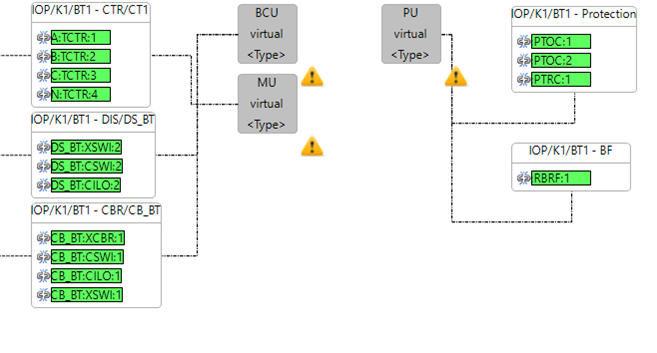
Figure 27: BT1 Function Specification
Communication Specification
Communication exchange between IEDs can be specified as well in HELINKS STS. After implementation, the signals which are used in the exchange are updated to the ones for the IEDs’ data models. The “Applications” option from the dashboard is used for creating application creation.

In the Applications section, users have the ability to specify peer to peer applications such as GOOSE and SV or client server applications such as MMS reports. After implementation of IEDs in the system, the communication can be configured and control blocks are created by Helinks STS. This guide contains instructions to creating GOOSE and SV applications. The report applications are to make customized report control blocks and data sets which are not necessary for this guide and so MMS specification is done by specifying inputs to a client which will be covered later in the guide.
Instructions
GOOSE and SV Application Specification
Table 4 shows all the GOOSE and SV applications used in this guide.
Table 4: IOP IED Communication
Publisher | Protocol | Application | Subscriber | IEC 61850 signal |
K1IncA1PUBCU | GOOSE | Breaker Failure | K1BT1BCU | BFR1.RBRF.1.ST.OpEx.general |
Protection GOOSE | K1BT1BCU | TRIP.PTRC.1.ST.Tr.general | ||
K1IncB1PUBCU | GOOSE | Breaker Failure | K1BT1BCU | CC.RBRF.1.ST.OpEx.general |
Protection GOOSE | K1BT1BCU | PH3.PTRC.1.ST.Op.general | ||
K1BT1PU | GOOSE | Breaker Failure | K1IncA1PUBCU | BkrFa.RBRF.1.ST.OpEx.general |
K1IncB1PUBCU | ||||
GOOSE | Protection GOOSE | K1BT1IncA1PUBCU | PhsToc.PTOC.1.ST.Str.general | |
K1BT1IncB1PUBCU | PhsToc.PTOC.2.ST.Str.general | |||
K1IncA1MU | SV | SVIncA1 | K1BT1PU | IAW.TCTR.1.MX.Amp.instMag.i |
K1IncB1MU | SV | SVIncB1 | K1BT1PU | IL1.TCTR.1.MX.AmpSv.instMag.i |
K1BT1MU | SV | SVBT1 | K1BT1PU | I01A.TCTR.1.MX.AmpSv.nistMag.i |
Open the Applications option from Dashboard.
Click on “GOOSE” use the right mouse click on “GOOSE Applications” and choose “New Application”.
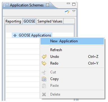
Figure 28: GOOSE new application
Name the application “Breaker Failure” and press OK.
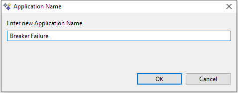
Figure 29: Breaker Failure new application
The application is made, and we have to specify the exchange. Use the right mouse click on “Breaker Failure” and choose “Open Application Editor”.
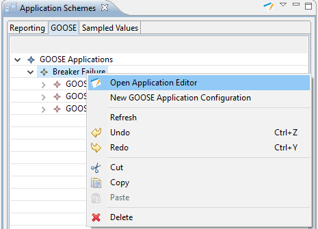
Figure 30: Open application editor for Breaker Failure
In the application editor, you can specify the publisher and subscriber functions from the options on the right-hand side of the screen. Click on “Sending Function” and choose the BF functions from IncA1, IncB1, BT1 according to the information from Table 5.
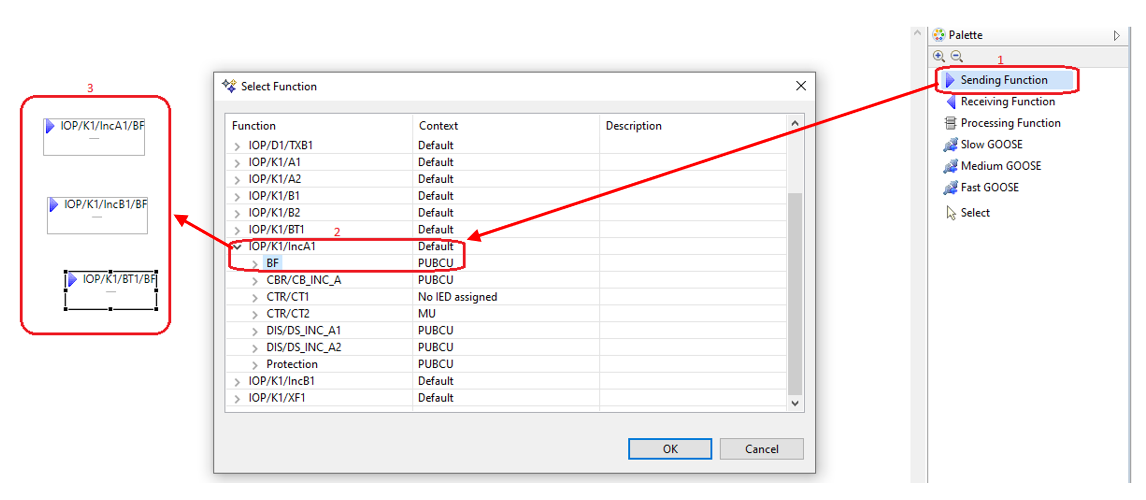
Figure 31: Specifying publishers
According to Table 4, the signal OpEx.general is being published. So, use the right mouse click on each of the sending functions and choose that signal.
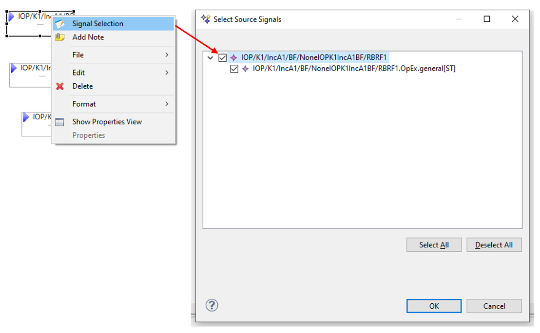
Figure 32: Specifying publishing signal
Specify the subscribers according to Table 4. As an example, the OpEx.general signal from the IncA1 and IncB1 protection function are being published to BT1BCU function. So, choose “Receiving Function” from the right side of the screen and choose the function CBR/CB_BT1.
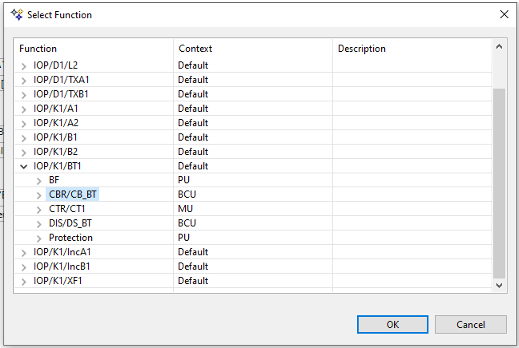
Figure 33: Receiving function
The recipient logical node would be the XCBR since the status of a breaker failing to open is being sent to other breakers in the substation. Choose “Fast GOOSE” on the right side of the screen.
Draw a line from OpEx.general in the IncA1 Protection function to the subscriber function. Another window opens which asks to specify the subscriber logical node. Choose XCBR.
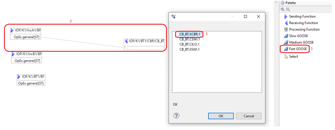
Figure 34: Draw from publisher to subscriber GOOSE
Next window asks for a name for the input signal to the XCBR. It can be the name of the publishing signal OpEx.general or it can be customized. You can choose the name IncA1.OpEx.general.
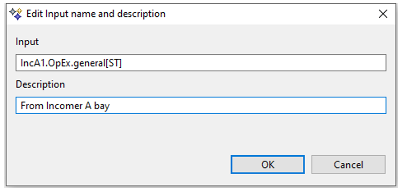
Figure 35: Input signal name
Do the same thing for the BF function from IncB1 and draw a line from OpEx.general to the CBR function as the subscriber and choose the name IncB1.OpEx.general as the input name.
The BF function of BT is publishing the OpEx.general signal to the CB functions from IncA1 and IncB1. So, create those subscribers and using the same method, create the line between the publisher and subscribers. You can choose the name “BT1.OpEx.general” as the input name. You can use the “Arrange all” button to arrange the publishers’ and subscribers’ functions.
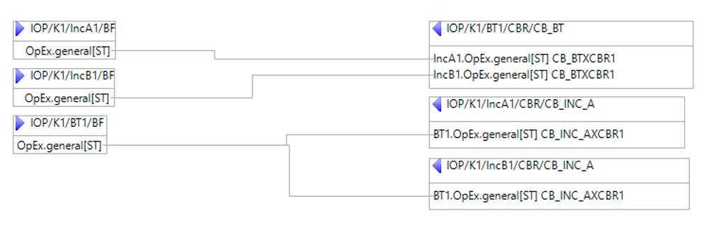
Figure 36: Breaker Failure application
According to Table 4, there is another GOOSE application called Protection GOOSE. Create the application and the publishers and subscribers accordingly. Choose the correct signals for publishers.
Draw the line form publishers to subscribers. The receiver for PTRC signals is the XCBR logical node from the CB function of BT1BCU IED. The receiver for PTOC signals from the Protection function from BT1PU is the PTOC logical node from the Protection function of IncA1PUBCU and IncB1PUBCU IEDs. The PTRC tripping signal is sent to inform breakers to open. The PTOC operate signal is sent to other bays to block their protection signals.
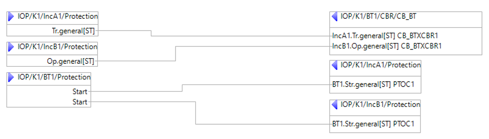
Figure 37: Protection GOOSE Application
From Table 4, it is seen that there are 3 SV applications, one for each bay, in this communication exchange. Follow the same rules for GOOSE, create a new SV application with the name SVIncA1.
Choose the CT2 function from IncA1 bay as the publisher. This is the function which has the MU IED assigned to it.
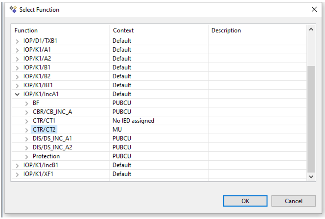
Figure 38: Publisher for SVIncA1
Choose the AmpSv.instMag.i from one of the TCTR logical nodes. Normally, all four signals are being published to cover three phases and the neutral but to expedite the process, we only send one signal.
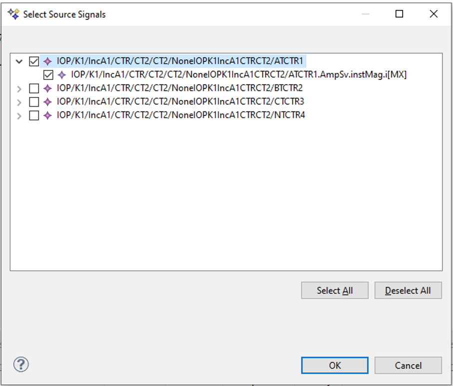
Figure 39: TCTR signal as publisher
The subscriber is the protection function from BT1 bay. The receiver logical node is the PTOC since it is getting measurements from the current transformers from other bays. So, create the subscriber.
Draw a line from the publishing signal to the subscriber using SMV Configuration option from the right side of the screen. and choose PTOC. You can create an input name such as IncA1.
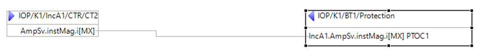
Figure 39: SVIncA1 application
Create two more SV applications and follow the same method for SVIncA1 and create the communication between publishers and subscribers according to the information from Table 5.
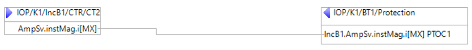
Figure 40: SVIncB1 application
Figure 41: SVBT1 application
Client-Server Specification
MMS report control blocks can be created and specified in Helinks STS. One method is to make customized applications using the same method for GOOSE and SV in the Applications section of the tool. Another method is to specify the input signals for the client from servers in the system and leave it to Helinks STS to configure the report control blocks and data sets. In this guide, instructions are given for the latter.
Client is specified as a virtual IED in the function specification diagram of the substation. So, open it for the substation IOP in the Single Line.
The functions which are specified in this space are related to human machine interface (HMI) which monitors the signals and network control center (NCC) which can give out control commands. The logical nodes in this space are interface logical nodes which start with the letter “I“.
Table 5: Substation Function Specification
Function | Logical Node | Virtual IED | Role | IED |
HMI | IHMI | HMI1 | HMI main | |
HMI_red | IHMI | HMI2 | HMI redundant | |
NCC | ITCI | NCC | Network Control Center |
Based on Table 5, Create three functions with the proper logical nodes. Then create virtial IEDs and assign them to the functions. Follow the same method for function specification for the bays.
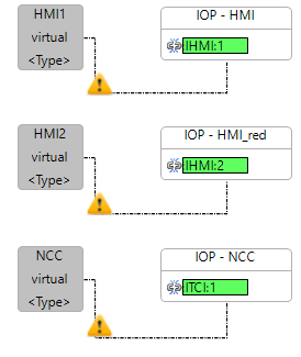
Figure 42: Substation Function Specification
As you have seen from Table 5, there are two HMI functions. One is the main HMI and the other is redundant. Click on the function “HMI_red“ and look at the properties at the bottom of the page. Change the “Redundant“ option from False to True.
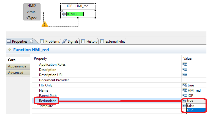
Figure 43: HMI Redundant
This way, you only have to specify input signals for one HMI function and the redundant one will follow it.
Use the right mouse click on HMI:1 logical node and choose “MMS Reporting Inputs“
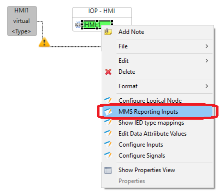
Figure 44: MMS reporting inputs
As you can see the screen is empty. Choose “Select“. Now you can choose the signals which are specified in the substation. You can choose to include all of them by clicking on the box next to the substation or next to the voltage level. Since in this guide, only three bays are included in the SAS, click on the box next to IncA1, IncB1, and BT1. As you can see, each voltage level shows the functions and signals for each logical node in each function.
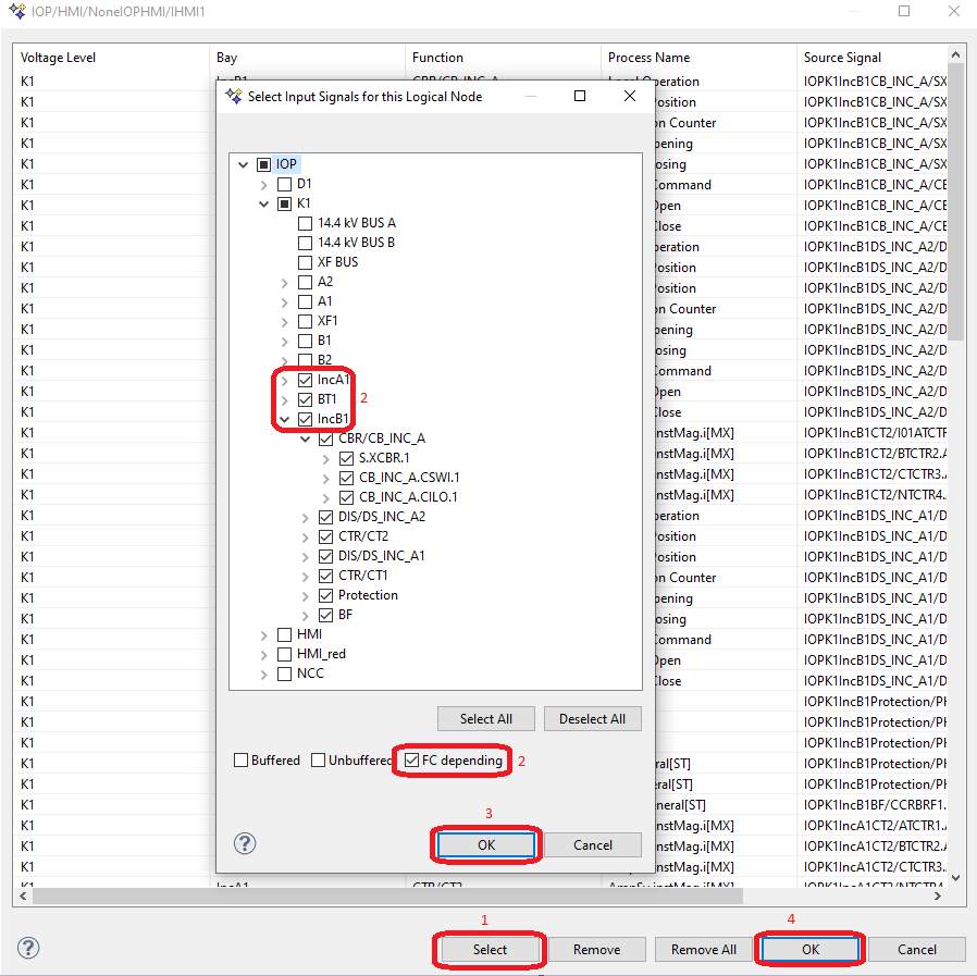
Figure 45: Specifying inputs signals
Once all the input signals are specified, Helinks STS will group them into data sets and report control blocks based on their respective Functional Constraints. All signals with the functional constraint ST are grouped to buffered report control blocks and all the signals with MX are grouped to unbuffered. From Figure 45, make sure the box “FC depending” is chosen, and press OK, press OK on the window which now should show all the signals you have chosen to close it.
Do the same for the logical node NCC.
Specification phase is finished, and the next phase will be Integration.
System Integration
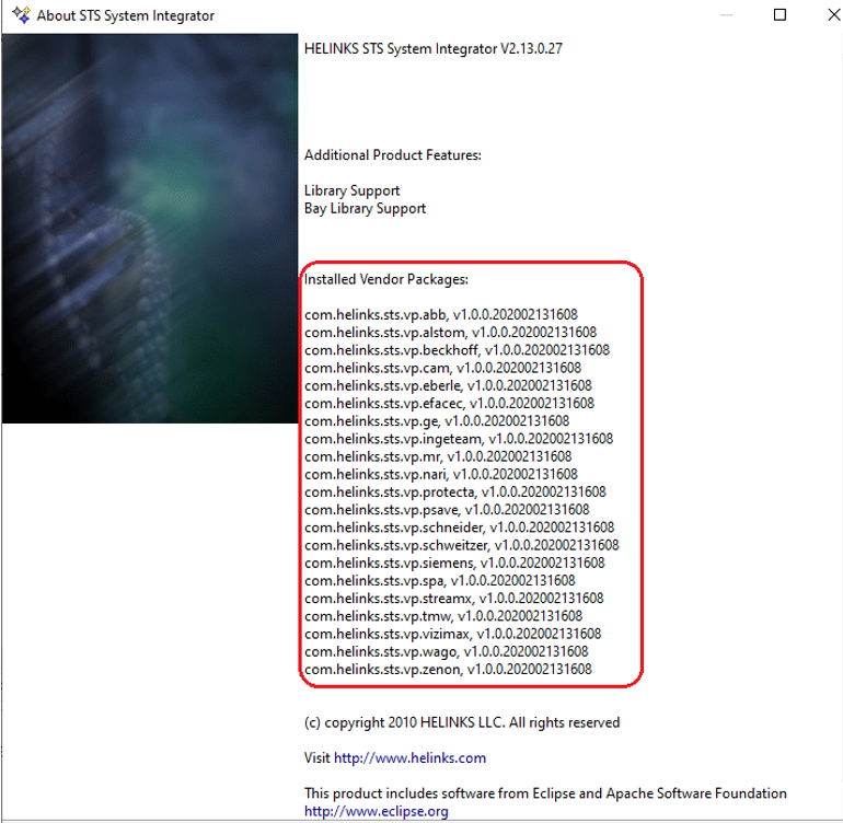
Integration phase of the design is about implementing real devices following the specification. Helinks STS supports IEDs from different vendors through the installation of vendor packages which can be viewed by opening “Help - > About STS System Integrator“.
Import SCL files
Integration for the IOP SAS design starts by importing SCL files of IEDs to the system. This is done by the Import functionality in Helinks STS.

If the SAS design is being driven by the specification, then there is no need to configure IEDs on their ICTs and so the ICD file which is for a template IED can be imported. This is the case for the IOP SAS Integration.
Table 6: IOP IEDs
Bay | IED name | IED type | IED role (virtual IED) | IP Address |
IncA1
| K1IncA1PUBCU | SEL 451 | Protection/Control Unit (PUBCU) | 10.10.10.1 |
K1IncA1MU | ABB SAM600 | Merging Unit (MU) | 10.10.10.2 | |
IncB1 | K1IncB1PUBCU | ABB RED 670 | Protection/Control Unit (PUBCU) | 10.10.11.1 |
K1IncB1MU | ABB SAM600 | Merging Unit (MU) | 10.10.11.2 | |
BT1
| K1BT1BCU | ABB REF 615 | Control Unit (BCU) | 10.10.16.1 |
K1BT1PU | GE D60 | Protection Unit (PU) | 10.10.16.2 | |
K1BT1MU | ABB SAM600 | Merging Unit (MU) | 10.10.16.3 |
Table 6 is a list of IEDs which are going to be used in the IOP SAS design. The IEDs are chosen based on their data model which needs to be according to the function specification. The IED name is chosen based on a common rule in IEC 61850 naming: “VoltageLevel/Bay/IEDrole”
Table 6 shows the IEDs are from three manufacturers. Three ICD files are already imported, and the instructions are to import the remaining two ICD files to the system.
Instructions
Click on Import from the HELINKS STS dashboard and choose the folder “ICD Files” from this directory which is made for you.
Two ICD files are used to import in this system: one is an ABB REF615 IED and the other is the SEL 451 IED.
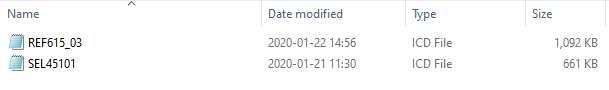
Figure 46: ICD files
Choose one of them and click on Open. Another window opens which is called the “SCL File Import Functions”. It recognizes the format of the SCL file and asks the user to choose an option accordingly.
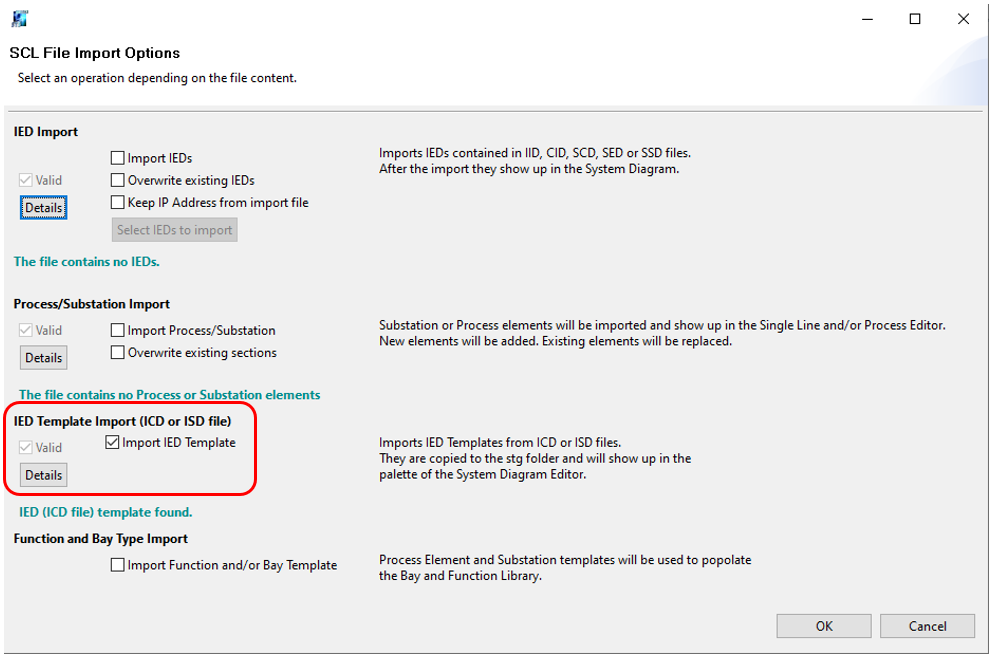
Figure 47: SCL import options
From Figure 47, the IED Import section is to import IEDs from CID or SCD files or any SCL file that has a configured IED. The Process/Substation Import section deals with the substation section of the SCD file and can import the single line diagram. The IED Template Import is used for ICD files. You can see it has found out the file which is being imported right now has a template of an IED.
Press OK on the SCL import options window and import the ICD file. You will see a window informing you the import has been successful.
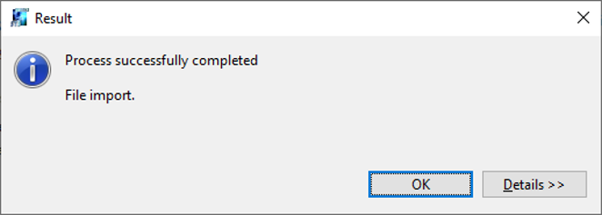
Figure 48: Import success
Import the other ICD file. Now it is time to instantiate the IEDs in the System Diagram.
System Diagram
After import of ICD files, they need to be instantiated meaning users need to create instances of the IEDs. In Helinks STS, System Diagram is the place to house these IEDs.

System Diagram is also used to create switches, create subnets and assign IP addresses to IEDs.
In System Diagram, users can create a Sub Network which will house all the IP addresses of IEDs. They can create generic devices such as switches, gateways, and even IEDs. By using the IED data model, logical nodes can be added to the generic IEDs and users can export their SCL file.
If ICD files with template IEDs are imported to the system, the IED is placed under its manufacturer.
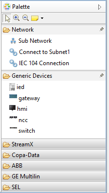
Figure 49: System Diagram options
Instructions
Open System Diagram by clicking on its icon from the Dashboard. On the screen, there are three switches which are created for the 3 bays. Some IEDs are already instantiated and are connected to their appropriate switches with the correct IP address. Particularly the HMI and NCC IEDs are already created. You can create instances of the rest of the IEDs from their ICD files and connect them to the switch for their respective bays.
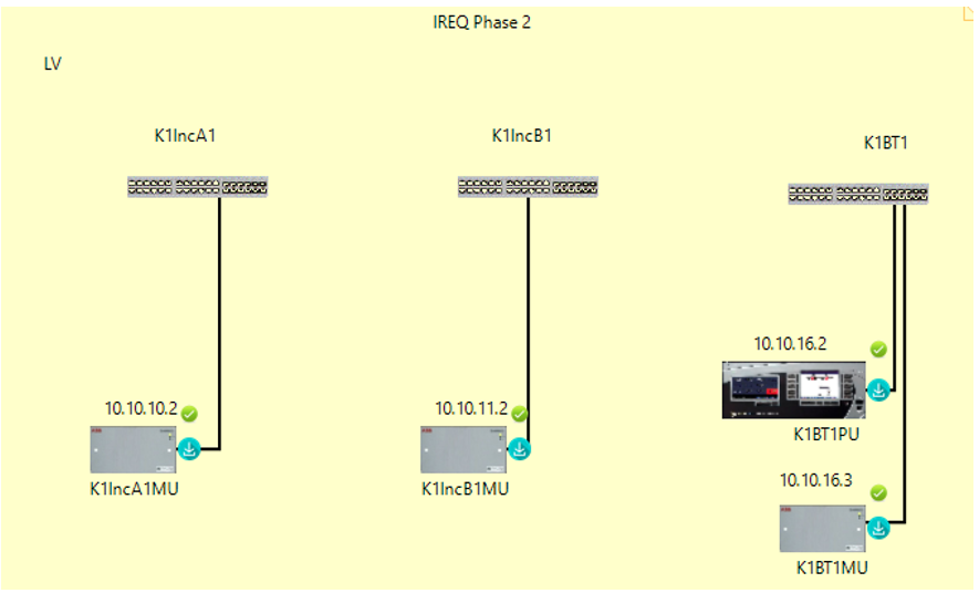
Figure 50: IEDs in System Diagram
Time to instantiate one IED. Open one of the manufacturer tabs for example ABB and SEL.
You can see there are 3 IEDs available under ABB including the REF615 one which you just imported. And there is only the SEL 451 which you imported under SEL.
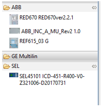
Figure 51: ABB IEDs in System Diagram
From Table 6, you know IncA1 has two IEDs. Click on the SEL451 under the SEL tab and click on the screen, preferably under the switch IncA1. A window opens to inform you the IED instance has been created successfully and the IED is instantiated with the name IED_1. You can change the name to K1IncA1PUBCU.
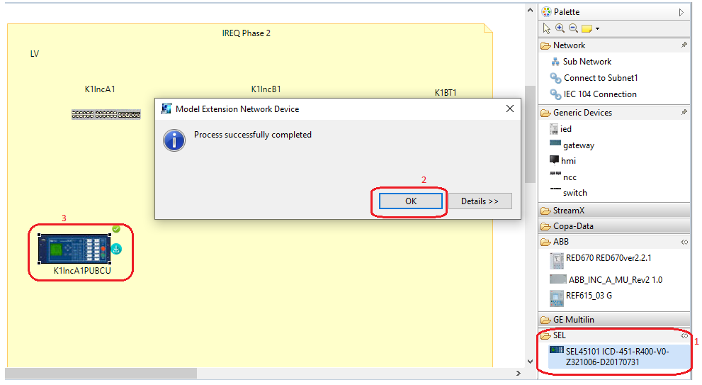
Figure 52: Create instance of SEL 451
From the right side of the screen, under the Network tab, choose “Connect to Subnet1”. Hover the mouse cursor on the IED. Hold the left mouse button and draw a line from the K1IncA1PUBCU to the switch K1IncA1. An IP address is assigned by default but change to the one specified in Table 6 which is 10.10.10.1 for this IED. This option enables you to connect the IED access point to the subnet with an IP address.
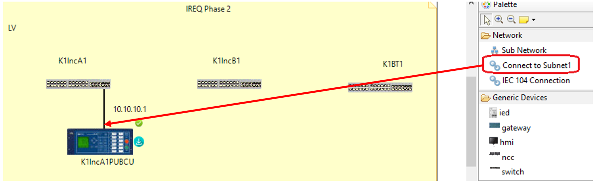
Figure 53: Connect IED to switch
If an IED has two access points, you are asked to choose one and you must choose the one which hoses the server and the IED data model.
K1IncA1PUBCU is connected to the subnet and you can verify it by looking at the IED Properties on the bottom of the screen.
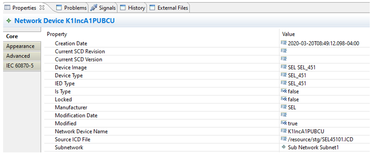
Figure 54: IED Properties in System Diagram
According to the information from Table 6, create instances for other IEDs and assign the correct IP addresses to them following what you just did for K1IncA1PUBCU.
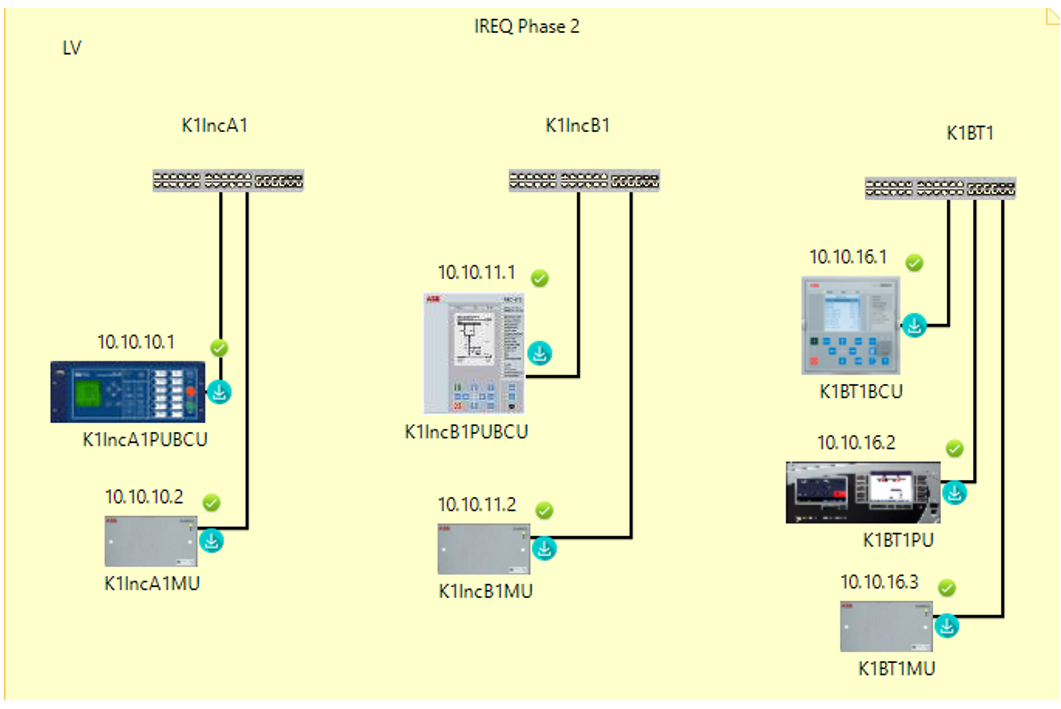
Figure 55: IEDs in System Diagram
IED Implementation and Logical node Mapping
Once IEDs are instantiated, they can be implemented to the virtual IEDs. Logical nodes can be mapped to the ones in the IED data models. This is done in the Function Specification Diagram for each bay. To speed up the process, the mapping will be done for the logical nodes which are being used in the communication exchange.
Table 7: Logical nodes used for mapping
IED | Function | Specified Logical Node | IED Logical Device | IED Logical Node |
K1IncA1PUBCU
| BF | RBRF:1 | PRO | BFR1:RBRF:1 |
Protection | PTOC:1 | PRO | P1:PTOC:1 | |
Protection | PTRC:1 | PRO | TRIP:PTOC:1 | |
CBR/CB_INC_A | XCBR:1 | PRO | BK1:XCBR:1 | |
K1IncA1MU | CTR/CT2 | A:TCTR:1 | CT1 | I01A:TCTR:1 |
K1IncB1PUBCU
| BF | RBRF:1 | PROT | CC:RBRF:1 |
Protection | PTOC:1 | OC4_1 | PH3:PTOC:1 | |
Protection | PTRC:1 | OC4_1 | PH3:PTOC:1 | |
CBR/CB_INC_B | XCBR:1 | CTRL | S:XCBR:1 | |
K1IncB1MU | CTR/CT2 | A:TCTR:1 | CT1 | I01A:TCTR:1 |
K1BT1BCU | CBR/CB_BT | XCBR:1 | CTRL | CB:XCBR:1 |
K1BT1PU
| Protection | PTOC:1 | Prot | PhsToc:PTOC:1 |
Protection | PTOC:2 | Prot | PhsToc:PTOC:2 | |
K1BT1MU | CTR/CT1 | A:TCTR:1 | CT1 | I01A:TCTR:1 |
Table 7 shows a list of all the logical nodes which will be used for mapping.
Instructions
Go back to “Single Line” by clicking on its icon on the Dashboard. Open the Function Specification Diagram for the bay IncA1. Use the right mouse click on the virtual IED PUBCU and choose “Implement”.
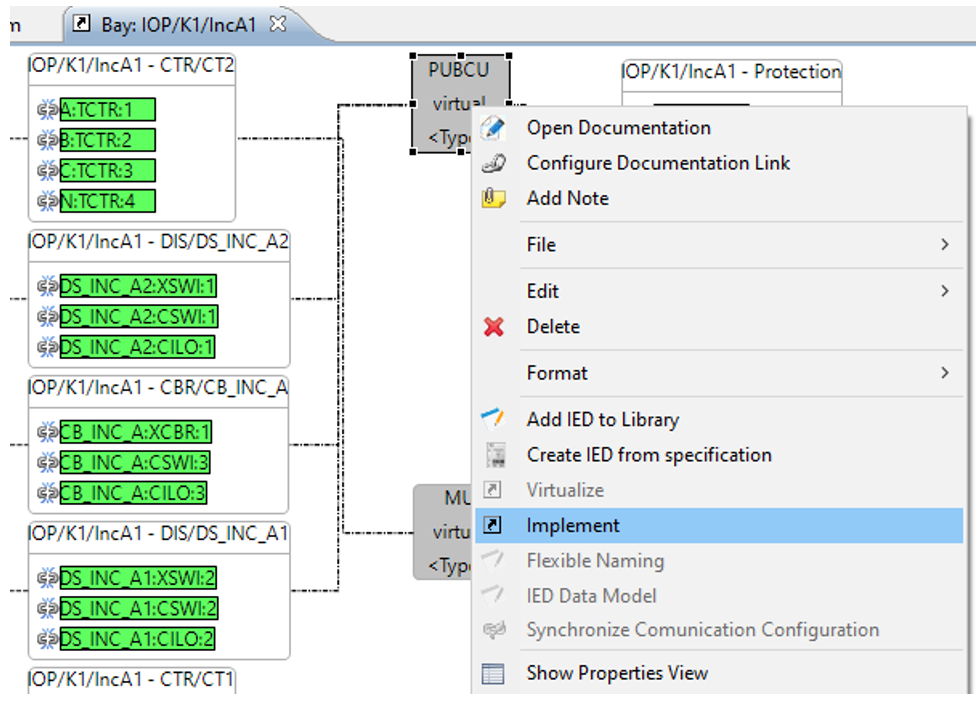
Figure 56: Implementing IncA1PUBCU
A window opens which shows all the IEDs that are instantiated to the system and are available for implementation.
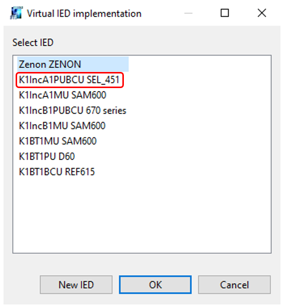
Figure 57: Available IEDs for implementation
Choose the IED K1IncA1PUBCU which is an instance of the SEL 451 IED. The virtual IED icon changes and shows the name of the IED in System Diagram and the manufacturer name.
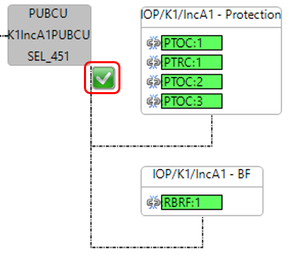
Figure 58: IED is implemented
Click on the highlighted icon from Figure 58. This opens the IED data model which can be used for logical node mapping.
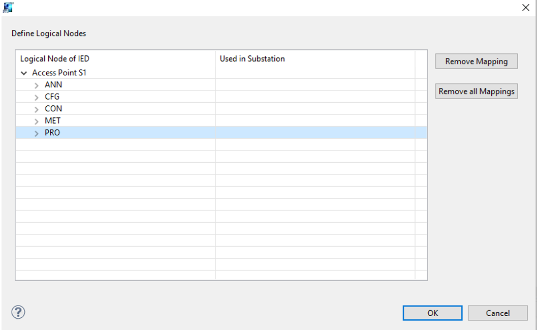
Figure 59: IED data model
From Figure 59, you can see the IED data model for K1IncA1PUBCU which is the SEL 451 device. The data model is categorized based on logical devices and each one has multiple logical nodes with different prefixes which are going to be mapped to those from specification.
Expand the “PRO” logical device. This LD has all the logical nodes which are needed for mapping in this bay. According to Table 7, find the P1:PTOC logical node.
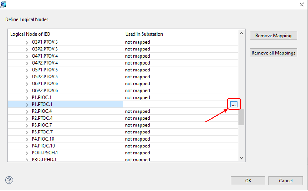
Figure 60: PTOC logical node for K1IncA1PUBCU
Click on field in the column “Used in Substation” in front of P1:PTOC:1 and click on the highlighted icon from Figure 60. This opens another window which shows all the specified PTOC logical nodes in the bay. According to Table 7, choose PTOC:1.
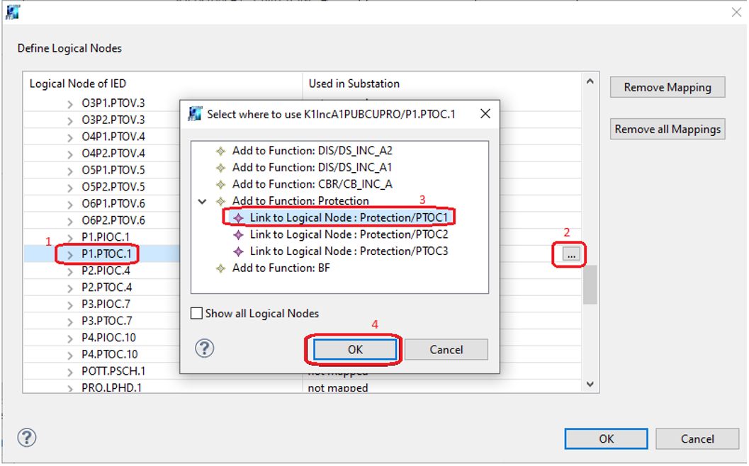
Figure 61: Mapping PTOC
The whole process is shown in Figure 61. Now the logical node is mapped.
Find RBRF, PTRC and XCBR in the same logical device and map them to logical nodes from the data model according to Table 7 with the correct prefixes and logical node instance numbers.
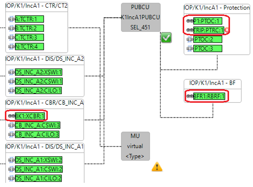
Figure 62: Mapped logical nodes for IncA1PUBCU
You can see from Figure 62 how the icons of the logical nodes which are mapped have changed. The logical node shows the prefix and logical node instance number of the IED data model and the chain icon next to the logical node has turned into a black linked chain. Signal list has also changed.
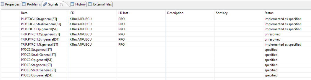
Figure 63: Signal list of mapped LNs
Figure 63 shows the signal list for the Protection function. You can see the signal status has changed for the PTOC:1 and PTRC:1 to “Implemented as specified”. Also, the IED column shows the name of the IED which is implemented, and the LD Inst column shows the logical device whose logical nodes are used for the mapping.
However, both Figure 62 and Figure 63 show a couple of signals for PTRC are unresolved. This is because the signal which is specified is not available in the signals for the PTRC from the IED data model. These types of signals can be deleted or mapped to another signal from another logical node or left alone.
Follow the same method and map logical nodes from the IED data models shown to the specified logical nodes for the rest of the IEDs in the three bays. Look at Table 7 as the reference. The table shows the logical device name for each IED and the logical node with the correct prefix and logical node instance number. You can delete the other logical nodes which are not mapped.
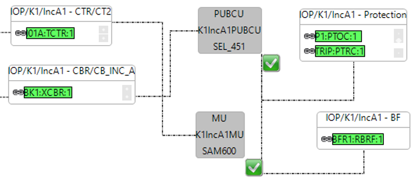
Figure 64: IncA1 mapped logical nodes
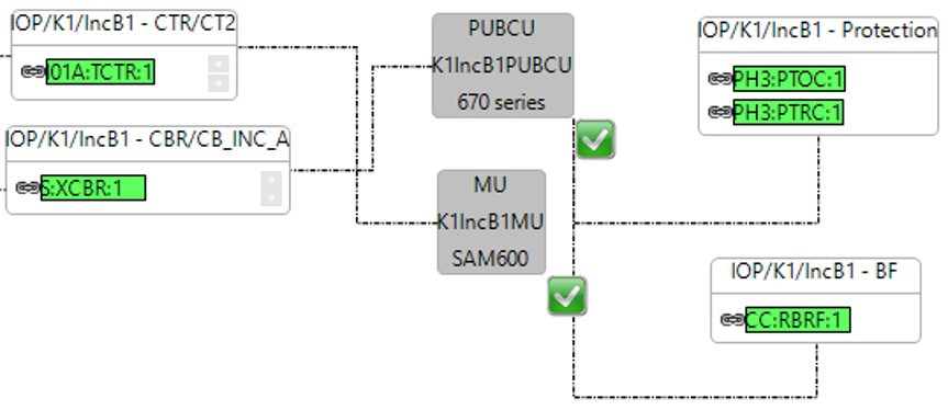
Figure 65: IncB1 mapped logical nodes

Figure 66: BT1 mapped logical nodes
You can delete the other logical nodes, remove the assignation of the IED to functions have unmapped logical nodes, and delete signals which are unresolved. But it will not make much of a difference. If a signal is unmapped or unresolved, it will not be added in the communication control blocks after communication configuration, which is the next and final step of Integration.
Part to show how to map the IEDs for the HMI and NCC.
Communication configuration, Validation, and SCD export
Communication Configuration: It means creation of control blocks for any communication application which has been specified. The “Set SCL Communication from Specification” option in HELINKS STS can create control blocks. Its icon can be found at the tool bar at the top of the page of the project.

Figure 67: Create Communication Configuration
Communication validation: It is done by opening Communication from HELINKS STS dashboard.
Communication Editor shows the details for communication applications which are configured which include data sets and control blocks.
SCD Export: Users can export the SCD file or SSD file by choosing this functionality from the HELINKS STS dashboard. A variety of options is available to customize the SCD file such as adding substation section to the file or excluding IEDs from the file.

Instructions
Communication Configuration
Click on the icon shown in Figure 67. The Communication Configuration Settings window will open.
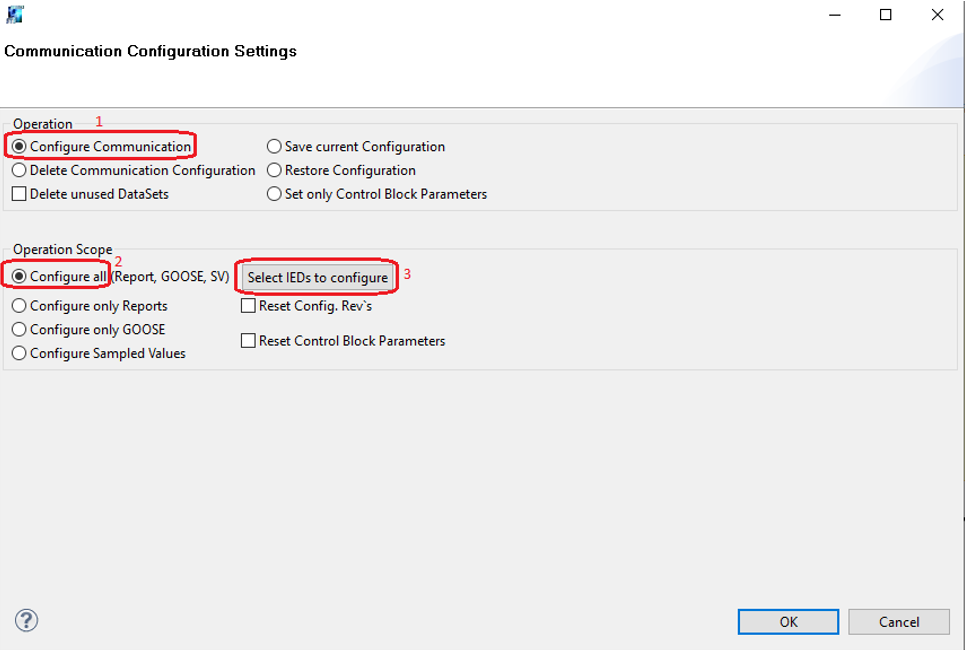
Figure 68: Communication Configuration Settings
There many options available in the settings shown in Figure 68, but the focus here is to configure communications. Choose “Configure Communication” option from “Operation”. Choose “Configure all” in “Operation Scope”. It means communication will be configured for all applications.
Click on “Select IEDs to Configure” on the settings from Figure 68.
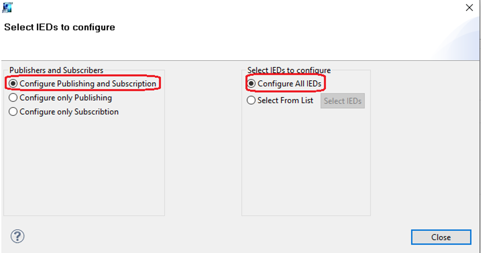
Figure 69: IEDs to configure
You have the option to configure only publishing, subscription or both as seen in Figure 69 and you can choose to configure communication exchange for all IEDs by using “Configure All IEDs” or for a few IEDs by choosing “Select From List”.
Choose the options “Configure Publishing and Subscription” and “Configure All IEDs”. And confirm the choices.
A prompt opens. Press Yes.
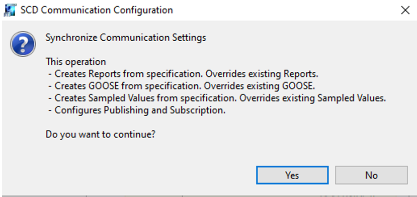
Figure 70: Communication configuration prompt
A message will show that the communication has been configured successfully.
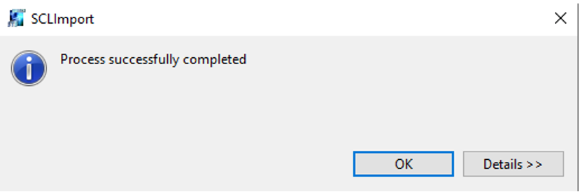
Figure 71: Successful communication configuration
Communication Validation: GOOSE and SV
You can validate the communication configuration by opening the “Communication” from the Helinks STS Dashboard.
You are seeing the Communication Editor now. Find the GOOSE Matrix tab.
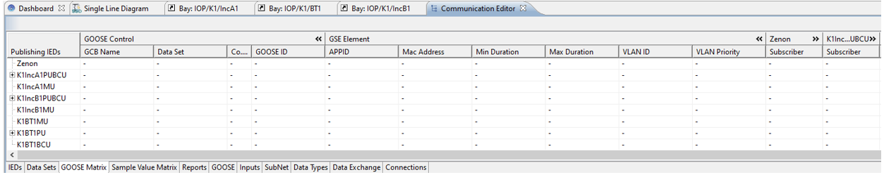
Figure 72: Communication Editor, GOOSE Matrix
GOOSE Matrix visible in Figure 72 displays the details for GCBs such as the GCB name, Data Set, GOOSE ID, MAC Address, etc for GOOSE publishers. Also, the subscribers for each publisher are indicated.
Expand the window for K1IncA1PUBCU to view its details.
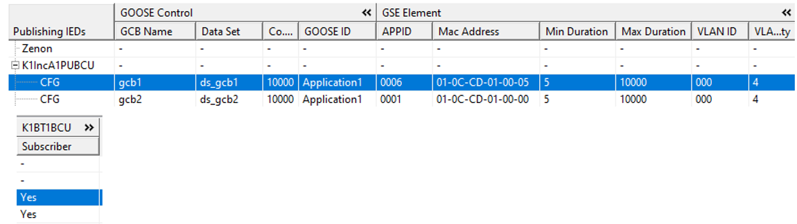
Figure 73: K1IncA1PUBCU GCBs
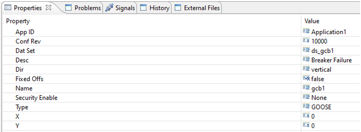
Figure 74: gcb1 properties
By looking at Figure 74, you can see the details for the GCBs for K1IncA1PUBCU and that the subscriber to both of the control blocks is K1BT1BCU which is correct according the communication specification done before.
Figure 73 is the properties for gcb1 which shows it is for the GOOSE application Breaker Failure. Both figures show the GOOSE ID (or App ID) is Application 1. This is the default GOOSE ID which is made by Helinks STS.
Change the GOOSE ID to: BF for gcb1, Protection for gcb2. In the properties for gcb1, click on Application1 and write BF.
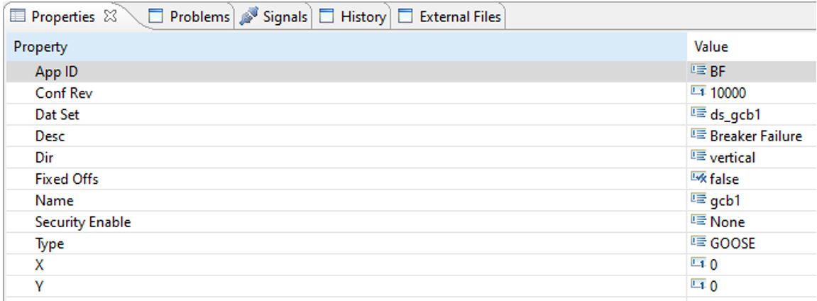
Figure 75: differnet GOOSE ID for gcb1
Expand the publishing details for the other publisher IEDs and verify the communication. You can also change the App ID or GOOSE ID to something you would like.
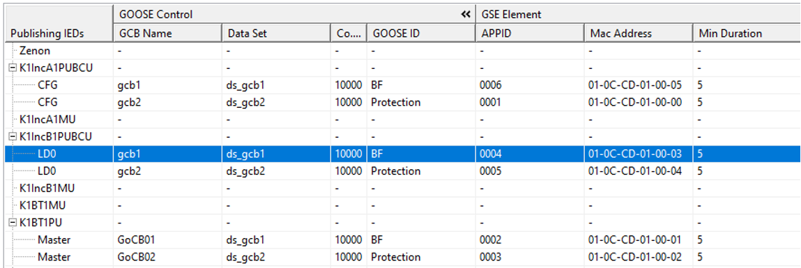
Figure 76: GCB details
Click on the SV Matrix tab in the Communications Editor. You can also see the details for each SVCB and the subscriber to publishers.
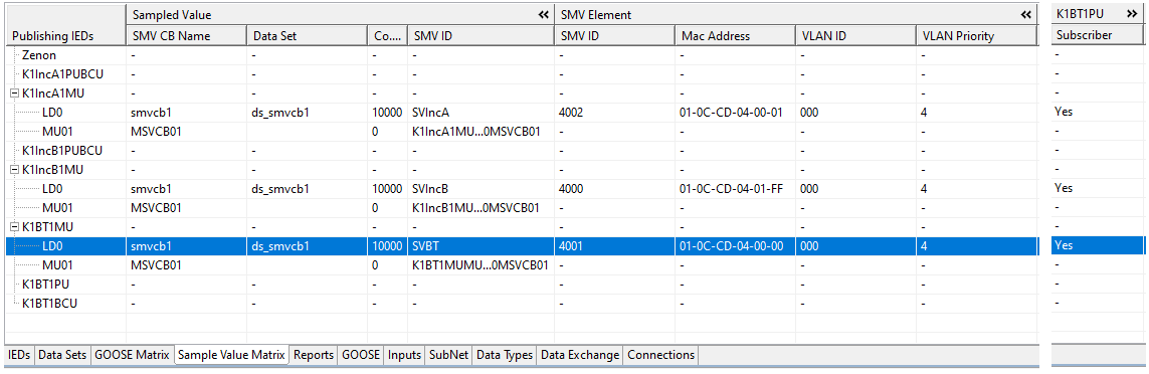
Figure 77: SVCB details
Figure 77 shows that the subscriber for all of the SVCBs is K1BT1PU which is what is specified in the section 4.3 of the guide. Also, the SMVIDs are changed to reflect the names of the SV applications.
Communication Validation: Report Control Blocks
From the same Communication Editor, open the “Reports“ tab. Here you can see all the report control blocks which are created for the servers which you specified before. You can verify the report control blocks along with their trigger options, client names, and optional fields in the Reports section of the communication as shown in Figure 78.
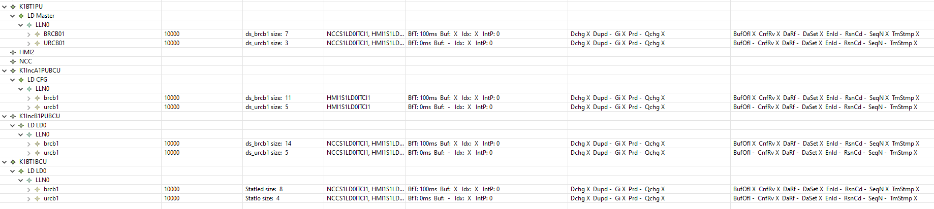
Figure 78: Report Control Blocks
SCD Export
Lastly, open the SCD export from the HELINKS STS dashboard.
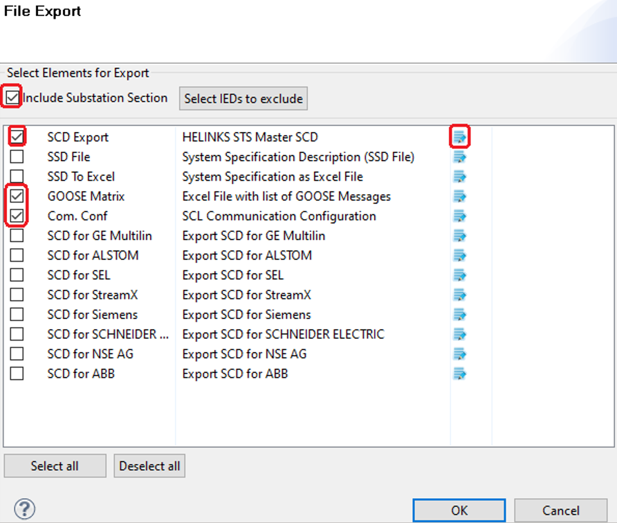
Figure 79: SCD Export
Choose to include the Substation Section on the SCD file from this project.
Choose the SCD Export to export the master SCD file of the SAS design. You can also choose GOOSE Matrix and Com. Conf which will export the GOOSE matrix and communication configuration as excel sheets.
There is no need to exclude any IEDs from the SCD file, but that option is available to you if needed. Click on the icon next to the SCD Export to configure the SCD file.
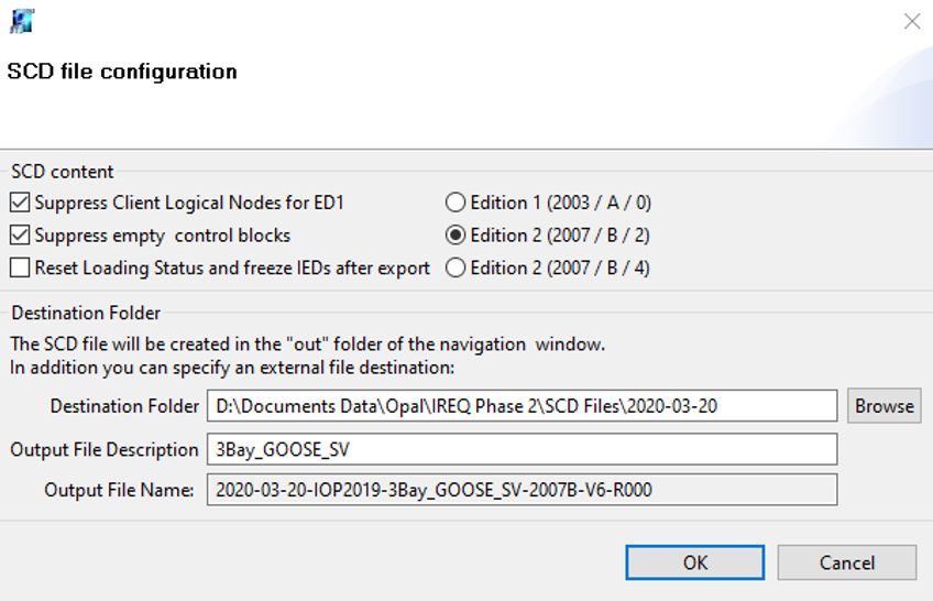
Figure 80: SCD file configuration
Like what you can see in Figure 80, choose a destination folder for the SCD file. You choose the name from the figure to be the name of the SCD file. The Edition 2 is chosen as the IEC 61850 edition of the file. Once everything is configured, press OK. Press OK again on the SCD File Export window.
Figure 81: Exporting SCD file
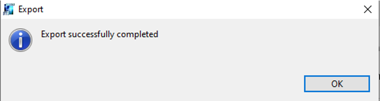
Figure 82: Export of SCD file successful
The SCD file is exported and you can check out the file in the destination folder. Or, you can view it and the excel sheets for GOOSE matrix and communication configuration in the “out” folder of the Navigator.
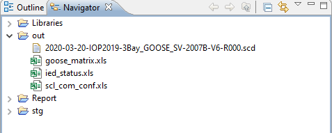
Figure 83: Output files in the out folder
Use the right mouse click on the SCD file and you can choose an outlet in which to open the file.
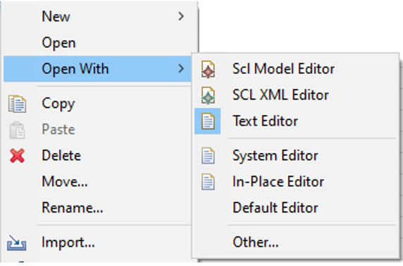
Figure 84: Opening SCD file
From Figure 84, the SCL Model Editor is like the Communications Editor and SCL XML Editor is like a tool like Notepad ++.
Choose SCL XML Editor
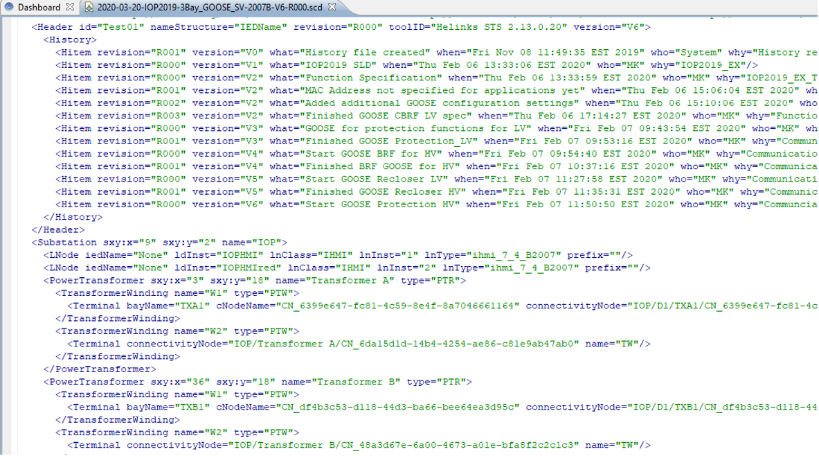
Figure 85: SCD File open in XML Editor
The Substation section is shown in Figure 85 so the substation section is included in the SCD file. You can also check out the control block parameters of the communication in the file.
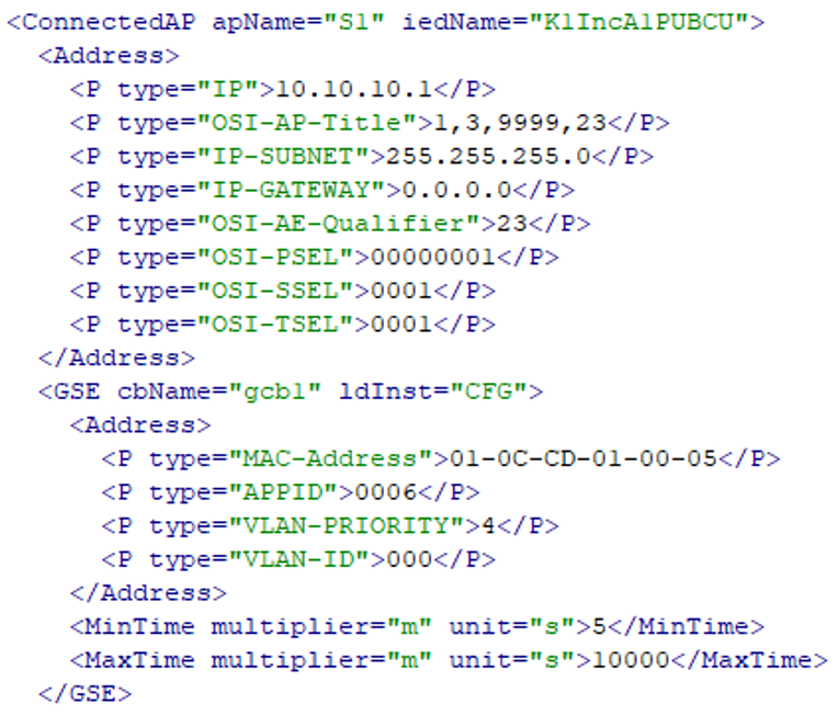
Figure 86: GCB in the XML Editor
Conclusion
By following the guide, new users of Helinks STS can create a basic substation automation system design based on IEC 61850 for an example substation.